Samsung a40 schematics galaxy fn sm Samsung galaxy a40 sm-a405f/fn/g schematics Samsung galaxy tab a 8.0 sm-t295 schematics
Samsung SGH E715 Schematic Diagram - RNB GAME - SHOP
Diagram samsung schematic sgh circuit e715 charger backlight power memory gr next Patrice benoit art: [45+] note 4 schematic diagram Motherboard mainboard circuit fm broadcom 3g
T295 sm schematics mainboard
Samsung galaxy e5 sm-e500h schematicsSamsung schematics manual 3/1/11 ~ mobile phone repair guidesSamsung sgh e715 schematic diagram.
.


3/1/11 ~ Mobile Phone Repair Guides

Samsung Galaxy Tab A 8.0 SM-T295 schematics
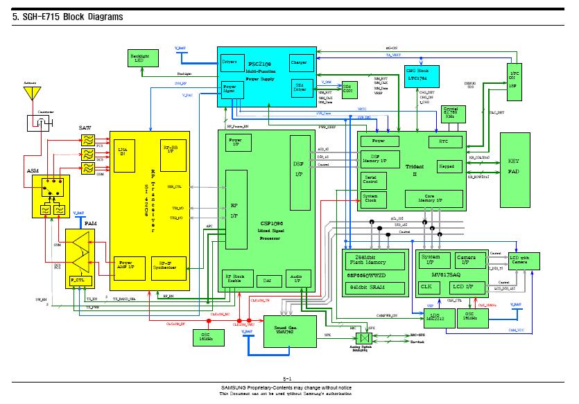
Samsung SGH E715 Schematic Diagram - RNB GAME - SHOP
![Patrice Benoit Art: [45+] Note 4 Schematic Diagram](https://i2.wp.com/image.jimcdn.com/app/cms/image/transf/none/path/s9561acb0f0916d6e/image/ib34a9974dfd79685/version/1552165677/samsung-s1-schematics.jpg)
Patrice Benoit Art: [45+] Note 4 Schematic Diagram

Samsung Galaxy A40 SM-A405F/FN/G schematics